In the field of computing, there are two foundational computer architecture models which define the basics of organization of computer components in a computer system. These architectures specify how memory, processing units and peripherals are organized in a processor.
Note
These architectures might not be used as it is but provide a reference to building an architecture for our embedded system. If you are familiar with the OSI Reference Model, then this trait would resonate with that concept.
The two architectures are:
1. Von Neumann Architecture (Princeton Architecture)
The von Neumann model is a result of the published work of John von Neumann in 1945, which defined the requirements of a general-purpose electronic computer.
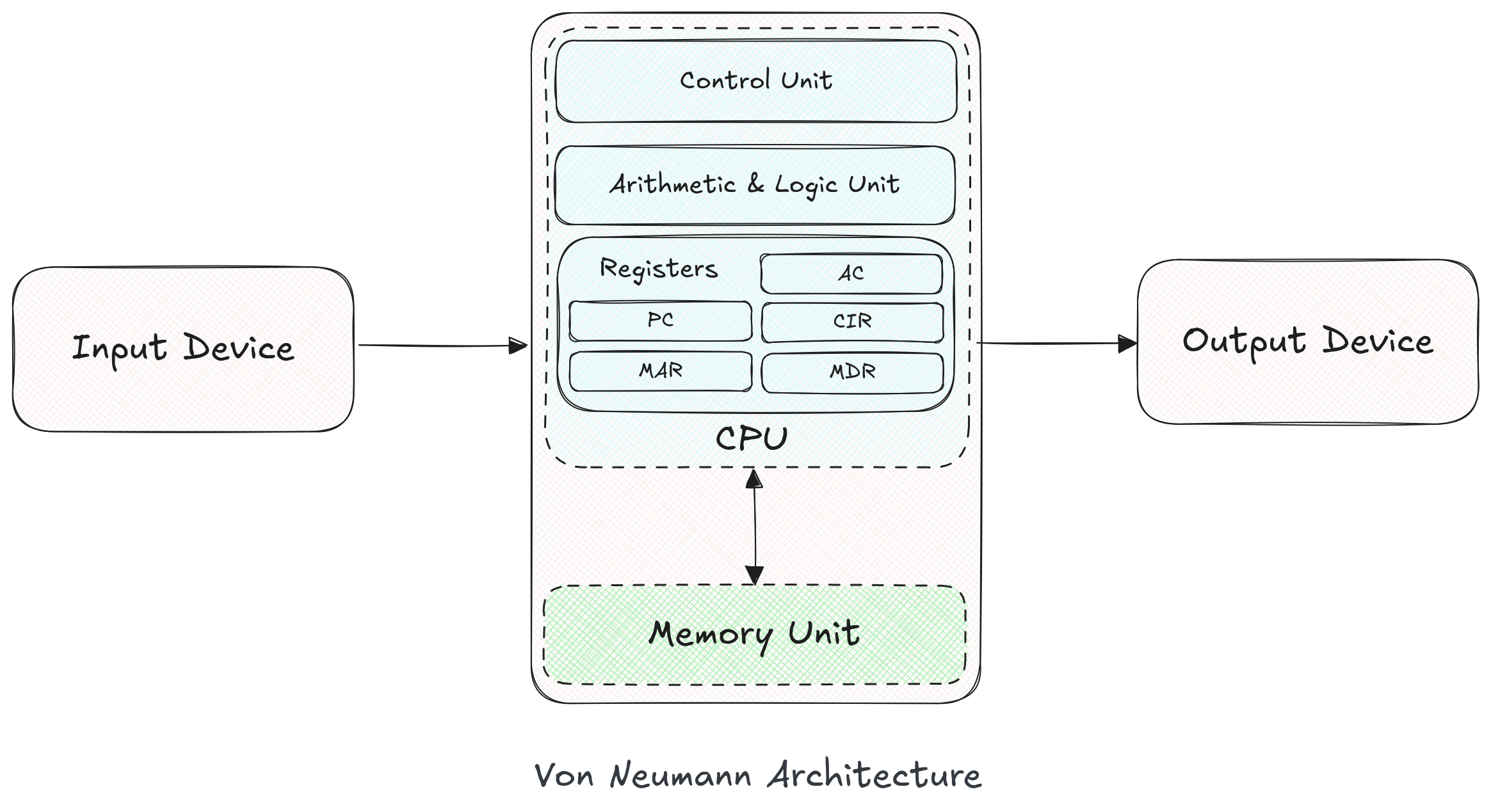 This model describes a computer system using following components:
- Control Unit
- Arithmetic & Logic Unit
- Registers
- Memory Unit
- Buses
1. Control Unit
The control unit is the heart of a computer system. It specifies commands to all other components to perform to carry out an operation. It controls the ALU, memory and I/O devices telling them how to respond to the program instructions it has interpreted.
2. Arithmetic & Logic Unit
There must be a method in computers to carry out arithmetic operations and the ALU provides means to perform these operations. The operations include arithmetic operations such as addition, subtraction, multiplication, and logical operations such as OR, AND, NOT.
3. Registers
Registers are high speed memory stores which are located inside the CPU. They are much faster than traditional memory devices and are used storing intermediate results. They also provide means to track addresses of various structures such as stack, program line, etc.
Von Neumann Architecture specifies 5 fundamental registers to implement a minimal computer system, namely:
- Accumulator: It is a general purpose register utilized during calculations for intermediate result storage.
- Program Counter: The PC tracks the address of next instruction to be executed.
- Current Instruction Register: The CIR contains the current instruction to be executed.
- Memory Address Register: The MAR holds the memory address of the data to be fetched.
- Memory Data Register: The MDR stores the memory fetched from the MAR for further operations.
4. Memory Unit
The Memory Unit also called the Store, contains a RAM (Random Access Memory) or main memory. This store is faster than the secondary memory and is directly accessible by the CPU.
This RAM is split into sections evenly and each section is used to store data, each having a corresponding address to identify the section.
In von Neumann Architecture, a single memory is used to store both the instructions and data. They are logically seperated by bounds in the memory. Naturally, this monolithic architecture has a single channel/bus to transfer both instructions and data. This leads to the slowing down of system, called a bottle neck or more specifically, the von Neumann bottleneck.
5. Buses
Buses are the means by which data is transmitted from one part of a computer to another, connecting all major internal components to the CPU and memory.
A standard CPU system bus is comprised of a control bus, data bus and address bus.
| Bus Type | Role |
|---|---|
| Address Bus | Carries the addresses of data (but not the data) between the processor and memory. |
| Data Bus | Carries data between the processor, the memory unit and the input/output devices. |
| Control Bus | Carries control signals/commands from the CPU (and status signals from other devices) in order to control and coordinate all the activities within the computer. |
Key Concept
One memory for both data and instructions, leading to a bottleneck.
2. Harvard Architecture
Harvard Architecture was originally developed for signal processing in the Harvard Mark I computer during the 1940s. Unlike the Von Neumann model, this architecture physically separates instruction memory and data memory, allowing parallel access to both at the same time.
.png)
This model describes a computer system using the following components:
- Control Unit
- Arithmetic & Logic Unit
- Registers
- Separate Instruction and Data Memory
- Dedicated Buses for Instructions and Data
1. Control Unit
Similar to Von Neumann, the control unit in Harvard Architecture is responsible for coordinating operations between the CPU, memory, and I/O peripherals. However, in this model, the CU accesses instructions and data through separate pathways, improving instruction throughput.
2. Arithmetic & Logic Unit
The ALU performs all arithmetic and logic operations, such as addition, subtraction, bitwise AND/OR, and shift operations. It’s functionally the same as in Von Neumann, but benefits from faster memory fetch due to parallelism in memory access.
3. Registers
Harvard Architecture also makes use of CPU registers for:
- Storing temporary data
- Tracking instruction execution
- Managing function calls and stack data
Just like in the Von Neumann architecture, you’ll find:
- Accumulator
- Program Counter
- Instruction Register
- Memory Address/Data Registers (often split due to separate memory buses)
4. Instruction Memory and Data Memory (Separate)
A major feature of Harvard Architecture is its separate memory spaces for:
- Instruction Memory – Stores only the program code (machine instructions)
- Data Memory – Stores runtime variables and I/O data
This allows the CPU to fetch the next instruction while simultaneously accessing or modifying data, effectively doubling the bandwidth and removing the von Neumann bottleneck.
Because of this separation, data cannot be accidentally executed as instructions — improving system integrity and security in some cases.
Key Concept
Physically separate memory blocks and buses for instructions and data → simultaneous access → faster execution.
5. Buses
In contrast to the unified bus in Von Neumann architecture, Harvard architecture uses dedicated buses
| Bus Type | Role |
|---|---|
| Instruction Bus | Transfers instructions from instruction memory to the control unit |
| Data Bus | Transfers data between data memory and ALU/registers |
| Address Bus | Separate address buses for instruction and data spaces |
| Control Bus | Controls both data and instruction transfers |
This dual-bus structure enables instruction pipelining and often leads to higher performance in embedded systems and microcontrollers (especially in ARM Cortex-M, DSPs, and Harvard-like RISCs).
Von Neumann vs Harvard
| Feature | Von Neumann | Harvard |
|---|---|---|
| Memory Structure | Unified (Data + Instructions) | Separate (Data ≠ Instructions) |
| Memory Bus | One shared bus | Separate data & instruction bus |
| Speed/Throughput | Slower due to bottleneck | Faster due to parallel access |
| Program Security | Lower (code can be overwritten) | Higher (code/data split) |
| Typical Use | General-purpose CPUs | Embedded systems, DSPs, MCUs |
Modified Harvard Architecture
A Modified Harvard Architecture is a hybrid model that combines the best of both the Von Neumann and Harvard architectures. While it retains separate instruction and data memories internally, it provides a unified memory interface externally, especially from the programmer’s perspective.
Quote
“Von Neumann on the outside, Harvard on the inside.”
— A common way to summarize Modified Harvard systems, such as those in ARM Cortex-M processors.
Key Traits of Modified Harvard Architecture:
-
Separate Buses Internally: The CPU still fetches instructions and accesses data via separate buses, which allows parallel operation and increased throughput internally. This happens despite having a single memory unit, by implementing a cache inside the CPU. The cache memory stores frequently used instructions and data seperately providing two seperate channels to the CPU, internally.
-
Unified Memory View for the Programmer:
Despite physical separation, the system presents a single flat address space, much like Von Neumann. This means program and data memory can be read/written using standard load/store instructions. -
Instruction Fetch as Data (Self-Programming):
Code memory can be accessed as data, enabling features like:- In-application programming (IAP): The firmware can update its own flash.
- Bootloaders: Can copy and execute code from various locations.
-
Examples in Real Hardware:
Most modern microcontrollers (like ARM Cortex-M3/M4, AVR, and PIC) use this architecture:- Flash memory holds instructions but can be read/written as data.
- SRAM holds runtime data, with fast access via data bus.
- Unified memory map accessible via a Load/Store model.
Example in ARM Cortex-M:
In Cortex-M processors:
- Instruction fetches use the I-Code bus.
- Data accesses use the D-Code and System buses.
- But from the C/C++ programmer’s point of view, both reside in the same memory map.
Key Concept
The Modified Harvard Architecture bridges performance with flexibility. It enables embedded systems to execute efficiently while maintaining a simple, Von Neumann-like programming model.