The Address Map in ARM Cortex-M processors defines how the 32-bit (4 GB) address space is divided and accessed by the CPU. It plays a vital role in connecting the processor to various memories (like Flash and SRAM), system peripherals, and external devices.
Unlike traditional processors with separate address and I/O spaces, ARM Cortex-M uses a unified memory-mapped I/O model, where all resources — code, RAM, peripherals, system registers — are accessed through memory addresses using standard LDR and STR instructions.
Structure of the 32-bit Address Map
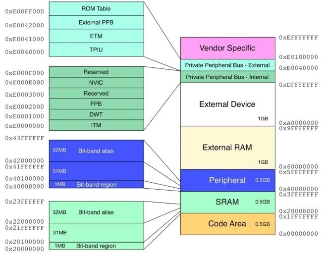
ARM Cortex-M cores (like M0, M3, M4, M7) use a fixed, standardized address map:
| Region | Instruction Access | Data Access | Bus Used | Executable | Description |
|---|---|---|---|---|---|
Code (0x0000_0000) | Yes (via ICode bus) | Yes (via DCode bus) | ICode / DCode | Yes | Flash or ROM for program code, vector table, and constants |
SRAM (0x2000_0000) | Yes (via System bus) | Yes (via System bus) | System (AHB) | Yes | On-chip RAM used for stack, heap, and data |
Peripheral (0x4000_0000) | No (typically not used) | Yes | System → AHB → APB | No | Memory-mapped I/O for UART, GPIO, SPI, etc., accessed via AHB-to-APB bridge |
| External RAM | Yes | Yes | System or external AHB | MPU dependent | Off-chip SRAM/SDRAM via external memory controller (e.g., FMC) |
| External Device | Yes | Yes | System or external AHB | MPU dependent | Off-chip devices such as Flash, LCDs, or sensors |
| Private Peripheral Bus | No (execute never) | Yes | PPB (dedicated internal path) | No | System control block, NVIC, SysTick, MPU, DWT, and debug modules |
| System Vendor Region | No (execute never) | Yes | PPB / Vendor-specific paths | No | Vendor-defined system-level extensions and debug interfaces |
1. Code Region (0x0000_0000 - 0x1FFF_FFFF)
-
Typically contains Flash memory or ROM.
-
Where the vector table and reset handler live.
-
May include bootloader or application code.
-
Supports execution and read access.
-
Can be aliased (e.g.,
0x00000000might map to flash even if flash starts at0x08000000).
2. SRAM Region (0x2000_0000 - 0x3FFF_FFFF)
-
Read/write memory.
-
Used for:
-
Global/static variables.
-
Stack and heap.
-
Runtime buffers, control structures.
-
-
Fast access (especially tightly coupled memory, if available).
-
Can include TCM (Tightly Coupled Memory) on M7/M33 variants.
3. Peripheral Region (0x4000_0000 - 0x5FFF_FFFF)
-
Used for memory-mapped registers of on-chip peripherals:
- UART, SPI, I2C, GPIO, ADC, Timers, etc.
-
Accessed via System Bus through an AHB-to-APB bridge.
-
Not executable — typically only read/write.
4. External Device Region (0x6000_0000 - 0x9FFF_FFFF)
-
For external memory-mapped devices:
-
External NOR/NAND flash
-
FPGAs
-
Parallel devices
-
-
May be connected through external memory controllers (like FMC/FSMC on STM32).
-
Not executable unless memory is configured correctly.
5. Private Peripheral Bus (PPB) (0xE000_0000 - 0xE00F_FFFF)
-
System control and debug features:
-
NVIC (Nested Vectored Interrupt Controller)
-
SysTick timer
-
SCB (System Control Block)
-
MPU (Memory Protection Unit)
-
FPU registers (if present)
-
-
Fixed addresses, standard across all Cortex-M cores.
6. Vendor Specific Region (0xE010_0000 - 0xFFFF_FFFF)
-
Reserved for vendor-specific use, advanced debug components.
-
Includes:
-
Trace macros
-
ETM, ITM, DWT (debug/trace tools)
-
JTAG/SWD access
-
Might not be accessible in lower-end devices
-